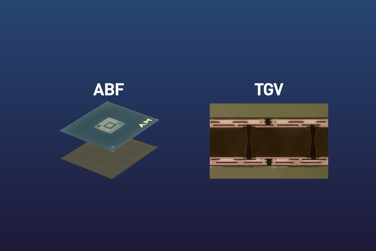
 ABF & TGV Substrate
ABF Substrate
- Body Size Max. 110 x 110mm
- Stackup Max.10+N+10
- Bulidup Layer Via/Pad Size (um) Min.50/75
- Bulidup Layer Line/Space (um) Min.8/8
- Bump Ptich (um) Min.90
TGV Substrate
- Sample build for 8+2+8 and above in Xiamen
- TGV diameter 100um and below
 BT Substrate
- 14L Anylayer with core / coreless structure
- Line/Spaces:
・Subtractive: 20/25 um
・mSAP: 12/18 um
・ETS: 12/12 um sample - 130um Pitch Flip-Chip CSP/BGA
- Sub-0.2mm 6L Core/Coreless substrates
- BT/FR5 Ultra low CTE, Low loss materials
- 2.5D cavity, Embedded pattern (ETS:Embedded Trace Substrates), Distributive buried capacitance and buried resistance layer
- Solder-on-Pad (SOP Technology within print and microball)


 Advanced HDI PCBs
High volume, reliable advanced HDI products
with up to 16 layer any layer
40/40um L/S
Fine pitch BGA
Up to 77G Hz High speed material hybrid HDI
Heavy Cu, Coin and novel thermal solutions
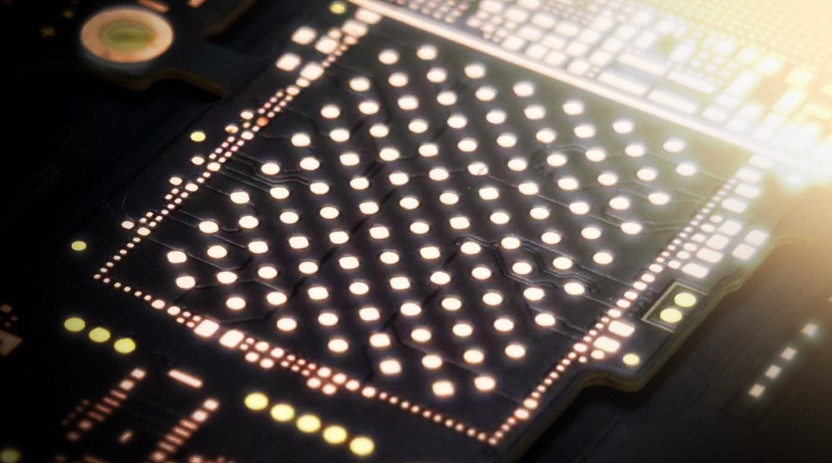
 Substrate-Like-PCB(SLP)
- 16L Anylayer
- 110um (Coreless) Min. Board Thickness
- 18/22 um L/S with mSAP
- Min. Flip Chip Pitch 127 um
- Next generation mainboard solutions for fine pitch, large I/O counts packages on mobile devices
- Cavity and 2.5D structures
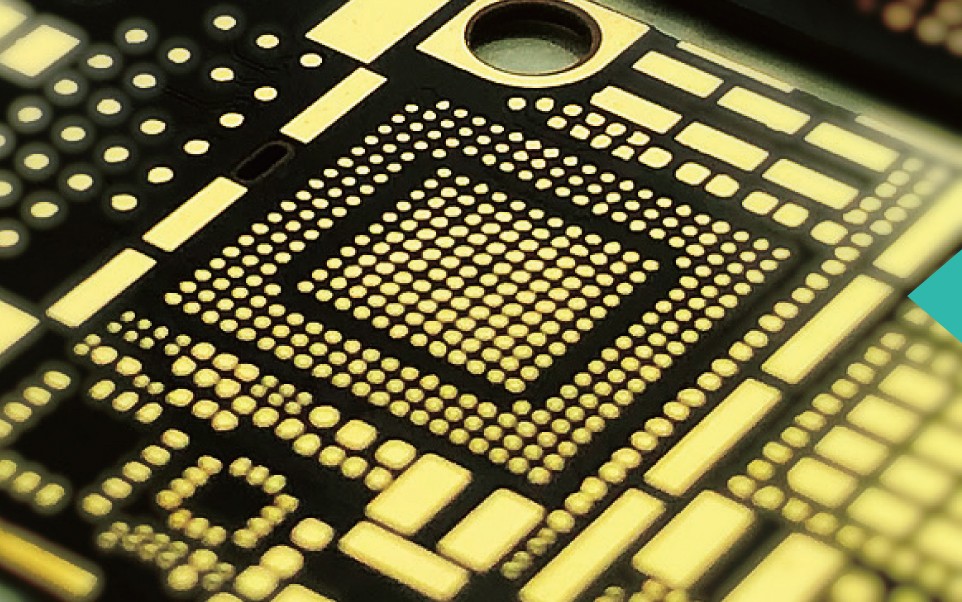
 SLP (Substrate-like-PCB) PCBs
High volume, reliable substrate-like-PCB
(SLP) products with Modified Semi-Additive (mSAP) technology
30/30um L/S
Fine pitch Fan-out Wafer
Level Package with large I/OS
 Advanced & Anylayer HDI & Rigid-Flex
HDI
- Up to 18L Anylayer HDI
- 30 /30 um L/S
- 0.3mm fine-pitch BGA
- Up to 77GHz high speed material hybrid HDI
- Cavity and 2.5D structures
Rigid – Flex
- Conventional PTH and Advanced/Anylayer HDl for Rigid-Flex PCBs w up to 10 flex layers
- 25 /25 um L/S
- 12um Pl, 10um coverlay ultra thin Rigid-Flex
- Pl and low loss mPl / LCP materials
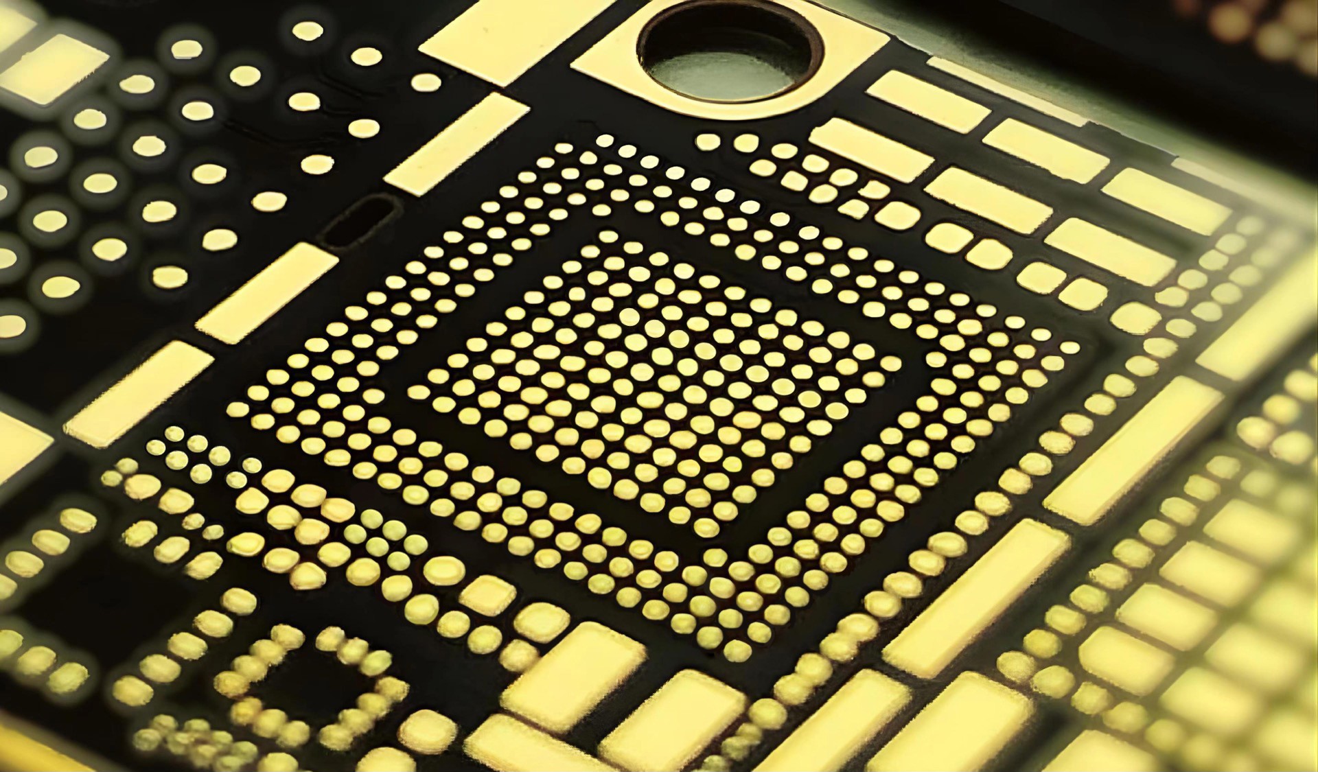

 IC Substrates
Ultra thin, highly customized module substrates
20/40um Subtractive, 20/30um mSAP L/S
150um Pitch Flip-chip CSP
<0.2mm 6L Core/Coreless substrate
BT/FR5 Ultra low CTE, Low loss, LED module Application Material
2.5D Cavity, Embedded Pattern, Distributive buried capacitance and buried resistance layer
Solder-on-Pad (SOP Technology)
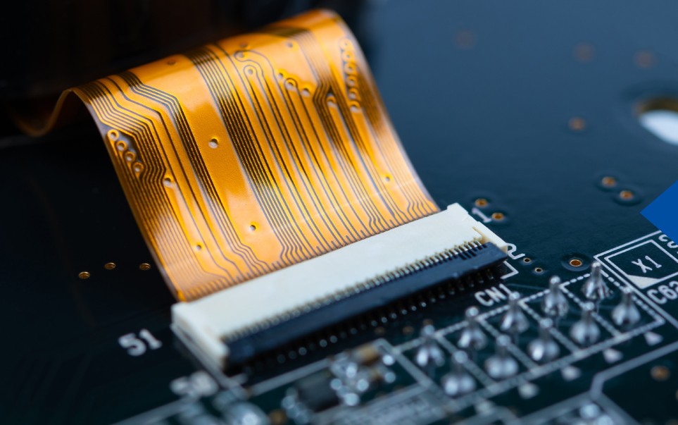
 Flex & Assembly
- 30 / 30 um L/S
- FPC Overall Board Thickness :0.036-0.8 mm
- 0.3 mm PIN Pitch (Connector & IC Chip)
- 0.35mm Pitch BGA/CSP/Flip chip
- PI and low loss mPI / LCP materials
- Flex-to-Install / Dynamic bend / Semi-Flex(Bending FR4 Flex)
- Symmetrical / Asymmetrical structures
- Component: 01005
 Power Battery Module (CCS)
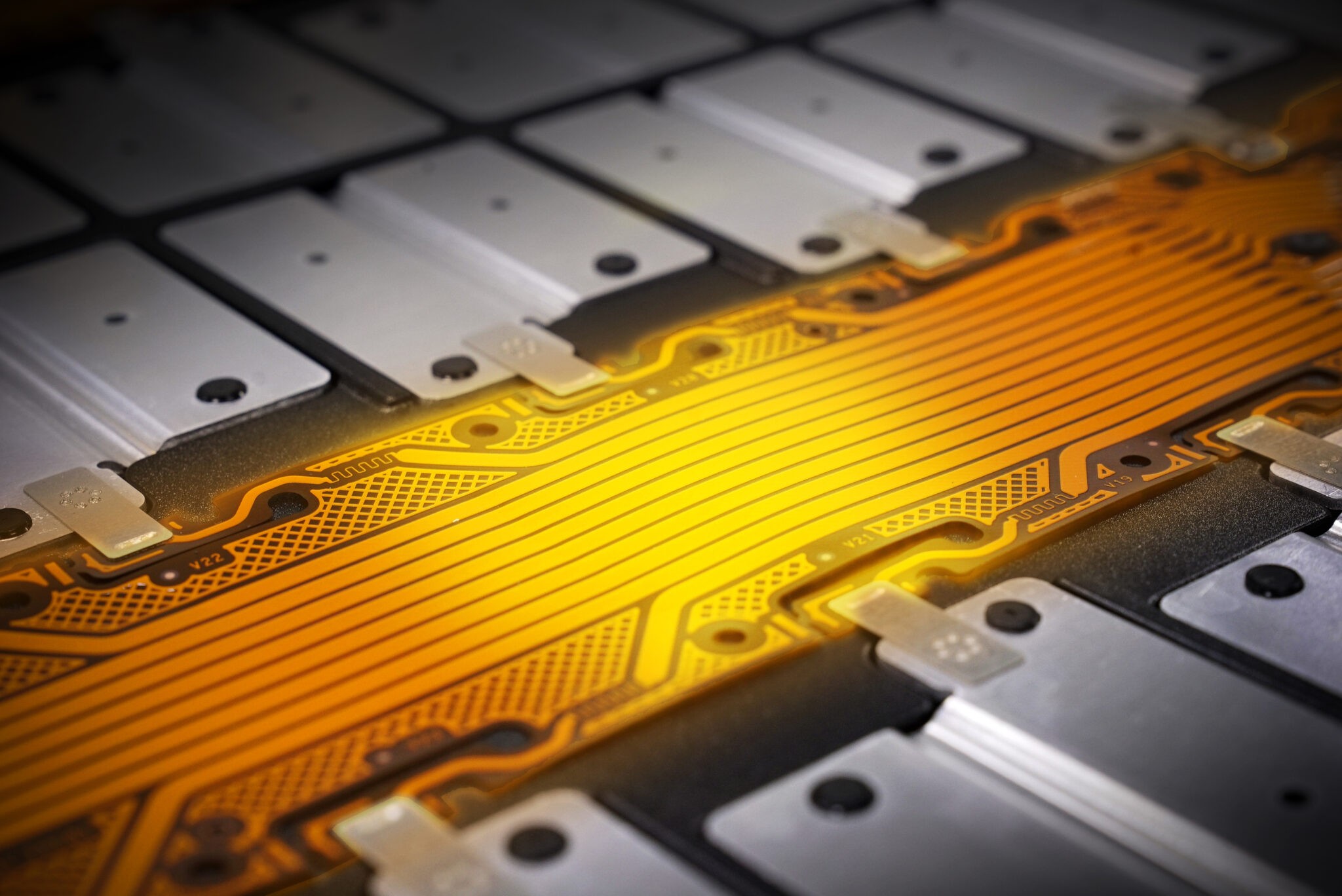
- Large panel size up to 2.4m for FPC and 2m for FPCA for temperature and voltage sensing and overcurrent protection
- Puncture crimp connector, Al/Cu ultrasonic welding
- PET insulation film lamination CCS, Hot riveting & injection molding CCS
- One stop-shop for design development, layout, simulation, fabrication, SMT, testing and assembly

 Flex / Flex-assembly / Rigid Flexible (HDI) PCBs
Flex, Flex-assembly, Rigid-flex
with advanced HDI / any layer technology
40/40um L/S
Fine pitch devices
12um PI, 10um Coverlay ultra thin thickness
Dynamic bend / Install bend / Semi-Flex
Symetrical/Unsymmetrical structures
PI and low loss PI/LCP materials
Customized assembly and testing

